Programmable Logic Design - I
Introduction
In labs 11 and 12 you built simple logic circuits on breadboards using TTL logic circuits on 7400 series chips. This process is simple and easy for small circuits. With increasing complexity of the logic circuitry the possibility of wiring errors grows and it becomes increasingly difficult to debug the circuit. Another problem is the difficulty in finding all the needed logic circuitry on available chips. To address these problems the electronics industry has developed the concepts of Programmable Logic Devices (PLD's) or Field Programmable Logic Devices (FPGA's). The basic idea behind these devices is the notion that logic circuitry of arbitrary complexity can be constructed from simple gates connected with appropriate links and the technical advance that has made this possible is the development of large gate arrays with computer programmable links. The design process then consists of specifying the logic design by means of a logic design language such as VHDL or by entering it on a schematic layout. A computer program then turns this design into a series of instructions that are downloaded into the chip to establish the desired logic circuitry. Facilities are provided to specify the pin out of the logic, to control placement of logic circuits on the chip and to impose timing constraints.
Design Tools
For our designs we will be using the Xilinx Corporation (www.xilinx.com) ISE Foundation 6.1i package along with the ModelSim Xilinx Edition II HDL simulation software. For reasons of lack of time we will restrict ourselves to Schematic Entry for our circuit description although the software supports a number of high level languages such as VHDL. We will sample only a few of the features and capabilities of this software package which is widely used in the electronics industry today.
Hardware
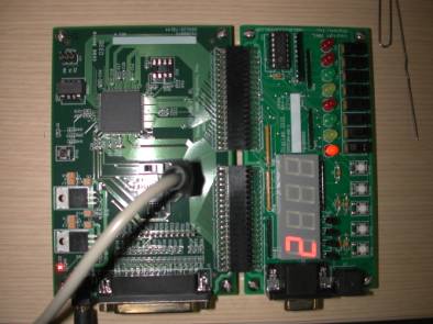
We will download our designs into a Digilab D2XL board connected to a Digilab Digital I/O board (DI01) shown in Figure 1 below. The FPGA chip on the D2XL board is a member of the Spartan II family, the XC2S30, embodying 972 logic cells with a total of 30,000 gates. While this size of device was state-of-the-art a couple of years ago, rapid advances in technology have pushed the largest device sizes to many millions of gates.
The D2XL board's I/O resources are limited to a single pushbutton and LED for use with a test program to verify proper operation. A large variety of I/O devices, however, are available on the DI01 board attached to the D2XL by means of two 40 pin connectors. Our two experiments will exploit the features of the D2XL/DI01 combination to design a number of circuits that will demonstrate the usefulness of this procedure.
Getting Started
Hooking up the Hardware
|
Figure 1: The D2XL and DI01 boards with programming cable attached. |
The circuitry is extremely delicate and can easily be destroyed if handled improperly. Static electricity which is easily generated is particularly dangerous and care must be taken to wear a grounded wrist strap when handling the circuitry. Your instructor will show you how to use it properly. Your two boards should be connected to one another, with power cord installed and a programming cable from the parallel port of the PC to the JTAG connector of the D2XL attached. Ask your instructor for help if this is not the case.
Testing the D2XL board
|
Figure 2: Project Navigator |
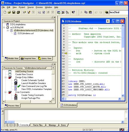
You should have a Project Navigator icon on your screen. Double click on it to open the program. As a first program to download we want to use "D2XLsimpledemo" to test the integrity of the D2XL board. If another project comes up, close it from the "File" menu and use "Open Project" from the same menu to open "D2XLsimpledemo". Ask your instructor for its location if you have trouble finding it. If you are successful you should get a screen display that looks like Figure 2 .
You need to double-click on the 3rd line in the top left window to get the display in the top right window. These five windows represent the design environment for the project with "Sources" in the top left window, the "Processes" for a given Source below it, the contents of selected files in the right hand window and text files below. Extensive help files are available online and at this time it would be a good idea to go to the "Help" window, select "ISE Help Contents" and then read the chapter "FPGA Design Flow Overview".
To test our board we are going to jump to the very last step in the "Processes" window which is "Configure Device [iMPACT]". Double clicking on this file name puts the program through all of the necessary steps to generate the file for downloading to the FPGA. This will happen, of course, only if there is no error in the intervening steps.
|
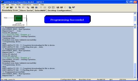
Figure 3: Successful Programming Result |
After you have done this you should get a "Configure Devices" window where you should select "Boundary Scan Mode" and next "Automatically Scan" and then "Finish". Click OK on the information box with "Boundary Scan Chain Contents Summary". The accompanying dialog should indicate that a cable connection was successfully established. Next select the "d2xlbtndemo.bit" file and click "Open". Right click on the xc2s30 icon in the graphic window, select "Program" and click "OK" on the next window. You should see an "Operation Status" bar indicating the progress of the programming and finally the screen in Figure 3 indicating that the device was successfully programmed. At this point LD1 (LD2 indicates that there is a power connection) should blink intermittently at ~3 Hz and by holding down the adjacent button you should be able to turn this intermittent blinking into a steady on state. If this is so, then the D2XL board is in proper working order and we can go on to our first project.
Troubleshooting suggestion: It may happen that in the programming process a) the cable is not identified or b) the programming may end in failure. Sometimes this happens if a previous design resides in the FPGA and has not been properly cleared. Remedies for this include starting the "Project Navigator" program over or interrupting the low voltage power to the FPGA board. Should you need to try the latter proceedure make sure that you are wearing a grounding strap so that you do not inadvertently destroy the device.
Design Project I
For our first project we will use "Schematic Entry" to design a circuit with a single AND gate. We will use "ModelSim" to test its proper operation, attach push buttons to the two inputs and an LED to the output. We will download it into the FPGA and test its operation.
Schematic Entry
Go to the Help>ISE Help Contents and read the chapter FPGA Design>Creating a Design>Creating a Schematic Project. Close the current project and select File>New Project to get to the Project Wizard. Choose a Project Name, Project Location on C disk (you should create a sub-directory with your name on C:\ where you will store all of your designs) and Schematic for Top-Level Module Type. Note that the appropriate hardware is selected and do not choose a Source File at this time. Select Project>New Source and Schematic for its type. Give it a name of your choosing. When the Wizard finishes, a schematic entry window is created. Click on the "Symbols" tab, choose "Logic" from the categories, click on the "and2" symbol and, using the mouse, place it in the schematic entry window. You may wish to magnify the drawing for better viewing. Next add input and output buffers to the two inputs and one output using the "buf" symbol which can be found under the "buffer" category. You will also need the wiring tool to make the connections. Each input needs an input marker and the output needs an output marker which can be generated by clicking on the I/O Marker icon on the toolbar at the top of the screen. Edit the default names to change them to In1, In2 and Out1 respectively. Save your design and go to Tools>Check Schematic to verify your design. If there are no errors you can go on to the next step. Your design should look like Figure 4 .
|
Figure 4: AND Logic Design |
Modeling the Design
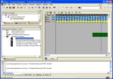
We must now model the design to see that it satisfies our design goals. Select Project>New Source>Test-bench Waveform and give it some appropriate name. Accept the default and you should get a Test-bench where you can with mouse-clicks select the logic levels for the two inputs to test all possibilities of the AND circuit. Save the file and you will see that a file of type .tbw is created, such as in Figure 5 . Select that file and in the Source page double click on "Simulate Behavioral Model". This will invoke the Modelsim simulation program and among the files produced you should get one that looks like Figure 6 below. Note that the time scale is given in ps and you will need to zoom out to see your logic signals which were on a ns scale. Verify that your design behaves properly. You should find that the truth table for an AND gate is faithfully reproduced.
|
Figure 5: The Test-Bench with input logic levels |
|
Figure 6: Simulation Results |
Assigning Pins
Next we must assign pins to our device. Checking the DI01 Manual we note on p.2 that the eight LED drive signals are active high. Thus we will attach the output of our AND to the drive signal of LED 1. On p. 4 we note that activating a pushbutton connects its output to Vdd or logic high. Thus we will want to tie our inputs to the outputs of pushbuttons 1 and 2. Next we check the DI01/D2XL pin correspondence chart and note that LD1 is connected to FPGA pin 93 and that BTN1 and BTN2 are connected to pins 84 and 85. Select the .sch file in the Sources window and double click "Assign Package Pins" under "User Constraints" in the "Processes" window. Answer "Yes" that you do want to create a .ucf file. In the .ucf file enter p93, p85 and p84 in the "Loc" column for I/O components "Out1", "In2" and "In1" respectively and then Save the file.
Implementing the Design
Select the .sch file in the "Sources" window and double click "Configure Device [iMPACT]" to generate the appropriate files and download them to the FPGA. Follow the same steps you did in the initial tests of the D2XL board. Ignore any warnings about clocks. You should once again see "Programming Succeeded" as the indication that no errors were found in your design and that the download was successfully accomplished..
Testing the Design
Manually verify that BTN1 and BTN2 are inputs to an AND circuit whose result is displayed in LD1.
Design Project II
|
Figure 7: A two-input NOR circuit constructed from NAND's |
Following the procedure above implement, simulate, download and test the circuit in Figure 7 which creates a NOR gate from 4 NAND's. You can once again use BTN1 and BTN2 for inputs and LD1 for the output. Verify that the truth table for a two-input NOR gate is satisfied.
Design Project III
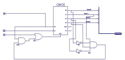
One of the huge advantages of this form of design is that macros of arbitrary complexity can be constructed, stored and reused in future designs. Our collection of symbols contains many such macros. For our next design we will use one of them, CB4CE, a 4 Bit Cascadable Binary Counter with Clock Enable and Asynchronous Clear, to construct a counter that will count from 0 to 9, reset and continue. We will then save it as a new macro to be used in our second experiment. The design we want to implement is shown in Figure 8.
|
Figure 8: A 0 to 9 counter |
Consider the logic diagram and prove that it does what we wish: count from 0 to 9 and then reset.
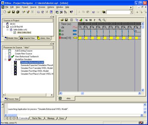
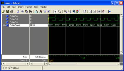
A new wrinkle in this design is the presence of a bus which is a collection of individual signals. It is automatically created when a wire, drawn with the wiring tool, is labeled as a vector e.g. btout(3:0). Individual elements of the bus are selected via bus taps with their names specified by using the netname tool. In our case these names are btout(3) to btout(0).Both sets of labels, of the bus and of the taps, must be in place or the program will not recognize the bus-tap connections. Create the schematic entry in Figure 8 , check for errors and save the file. The device that we wish to build will have 3 inputs, Ce for Clock Enable, Clr for Clear and Clk for Clock. Outputs will consist of a bus 4 bits wide, btout(3:0). Start a new project with schematic entry at the highest level. Enter your design in the usual fashion naming the inputs ce, clk and clr. To generate a bus for output draw a line using the wiring tool and give it a name btout(3:0). The program will change the line into a thicker, bus, line in correspondence with the name. Attach the bus taps as indicated and name them btout(0) to btout(3) using the "add net name" tool. Be sure to save the design and check for errors. If none are found go back to "Project" and create a new source of type "Testbench Waveform" using a single clock. Provide changes in the logic states of "ce" and "clr" to fully test your design. The page should look something like Figure 9 . Save this file and go to "Simulate Behavioral Model". Verify that your logic is working properly by examining the outputs on the "Wave" plot below (Figure 10 ). Note that the "btout" bus is given numerically after each clock transition.
|
Figure 9: Testbench Waveforms for Decimal Counter |
Next double click "Create Schematic Symbol" and go to the ECS page to create a symbol to represent your counter. Select "Tools" "Symbol Wizard" and opt for taking pin names from the drawing and a rectangular shape. Continue using the Wizard default values. Go back to the ECS page and verify that your new symbol is available for use.
We will need this macro for our second of two labs with FPGA's.
We will not download this design into our FPGA because we need a clock to drive it and the only clock available on the chip is a 50 MHz clock on pin 91. This runs much too fast for visual verification.We need to divide this rate down by a factor of several million but, we will leave that for next time.
