|
Wide Bandgap Semiconductors
Silicon Carbide
|
|
|
"Silicon Carbide (SiC) is no stranger to our universe, having been generated in the atmosphere of stars for billions of years. & hexagonal shaped microcrystals of SiC found in meteorites have their origin outside of our solar system..."
W. J. Choyke
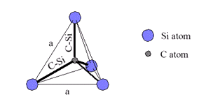
The wide bandgap semiconductor silicon carbide (SiC) is a fascinating material. In the single crystal form it is an indirect gap semiconductor with 2.38 < Eg < 3.26 eV (depending on polytype), which allows for electronic device operation to ~900 ° C. It is corrosion resistant to most acids and bases, and has a hardness of 9 (Mohs scale). The native oxide of SiC is SiO2, which we use to fabricate field-effect devices. I am interested in understanding the fundamental transport mechanisms of SiC field-effect structures and their application to chemical sensing in high temperature environments.
Phys. Stat Solidi 202 (1997) | |
|
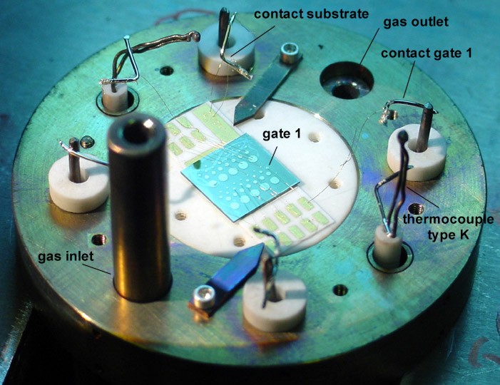
Photograph of an array of devices on a 1cm2 SiC substrate, prior to high temperature characterization in the furnace. Wire bonds connect each individual Pt sensor gate to a gold pad on the rectangular alumina header. In this system we can make four terminal electrical measurements of capacitance and conductance with pF and pA sensitivity up to 600 ° C in a controlled gas environment.
|
|
| |
|
SiC chemical sensors
[Back To Top]
Reducing pollution and improving energy efficiency require sensitive, rugged sensors that can quantitatively detect the gaseous products of combustion systems for automotive and energy plant applications. We are investigating the sensor response mechanisms of catalytic gate SiC devices for detection of hydrogen containing species. | |
|
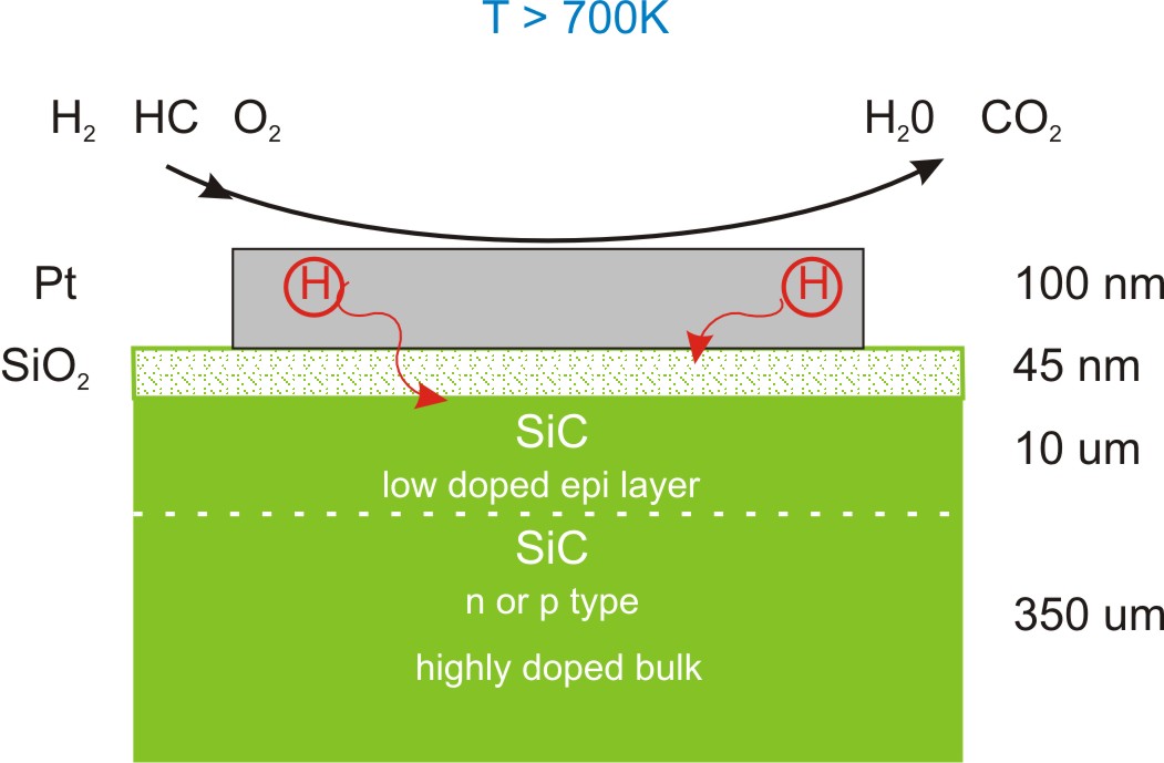
Schematic of a Pt - oxide - SiC catalytic gate sensor. The refractory metal gate de-hydrogenates long chain hydrocarbons at T> 700K. This chemical event is detected electronically as a change in the device potential.
|
|
|
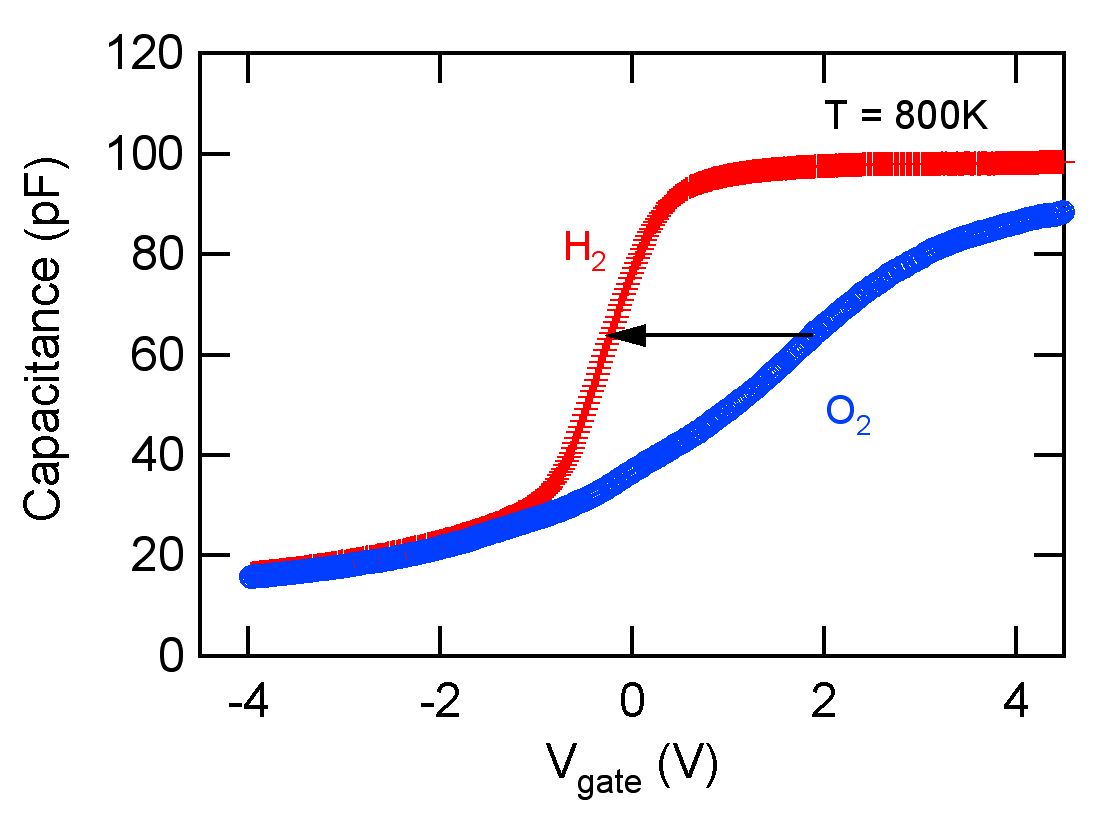
Capacitance-voltage characteristic (1MHz) of a SiC sensor at 527 ° C in hydrogen (10% H2 in N2) and oxygen (1% O2 in N2). For sensor measurements the capacitance is held constant, while monitoring the gate voltage during gas exchange. |
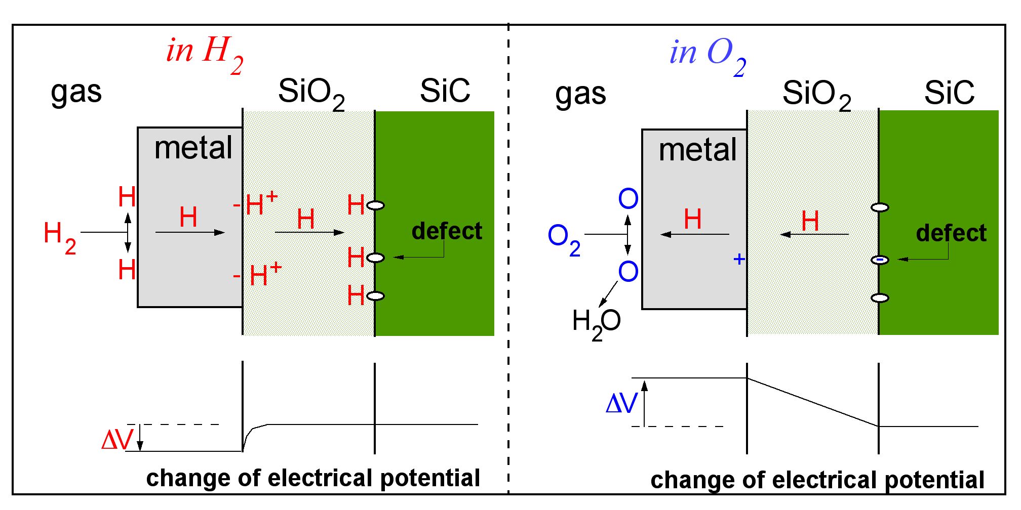 | |
Distribution of charge in the SiC sensor in hydrogen and oxygen. Two independent mechanisms are responsible for the sensor response: (i) chemically modified metal-semiconductor barrier height and (ii) charged states at the oxide - semiconductor interface. The latter mechanism may be significantly slower than the former, and can be minimized by biasing the device near mid-gap.
To probe further:
| |
|
Interface physics
[Back To Top]
We need to understand the mechanisms for charge transport in SiC structures operating under field conditions to design devices for applications such as high temperature electronics. For example, the "effective channel mobility of metal - oxide -SiC devices is significantly lower than that of the bulk Potential mechanisms for short range non-uniformity of the electrostatic potential at the SiO2 - SiC interface include: random distribution of charge (in the insulator or at the interface) and structural disorder in the SiC lattice at the interface. We are using a number of spectroscopic techniques to study this interface. | |
|
Charged states at the SiO2 - SiC interface
From quasi-static and 1MHz capacitance - voltage measurements of our SiC capacitors at elevated temperatures (up to 500K) we obtain the density of charged states at the oxide - semiconductor interface as a function of the position of the Fermi energy in the SiC bandgap. For 0.3 eV < Ec - E < 09 eV, the interface state density is 1 x 10¹¹ < Dit < 5 x 10¹¹ for our Pt - SiO2 - SiC capacitors. These values are comparable to 6H-SiC devices with standard gate metallizations such as Al or poly-Si. Note that these measurements represent a spatial average over the 100 - 400 μm diameter gate. | |
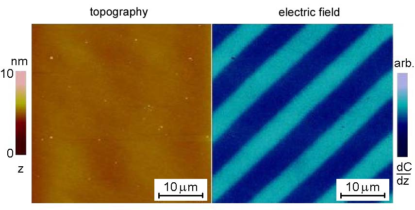
| Using scanning electric filed microscopy we have obtained spatially resolved images of the electrostatic potential at the buried oxide - semiconductor interface, without removing the gate oxide. Shown below are simultaneously obtained images of an oxidized Si sample implanted with 5 μm stripes of 6x10¹⁷ B/cm3 in a 1x10¹⁶ B/cm3 substrate. As expected the topographic image of the oxide is essentially featureless. The electric field image clearly resolves the dopant distribution of the bulk semiconductor. | |
To probe further:
Acknowledgements Thanks to our collaborators in this project:
Funding:

| |