|
A transformation is occurring in semiconductor technology, with the ultimate goal of developing devices based on manipulating the charge or spin of individual dopant atoms. Studying the physics of such minute systems is the motivation behind these experiments. |
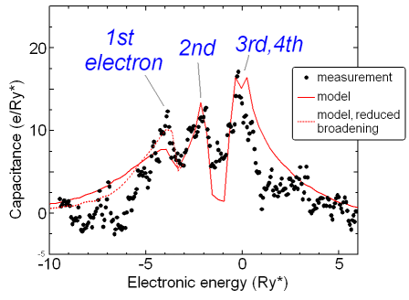
| Our experiments apply the Charge Imaging technique, which utilizes a charge sensor with a sensitivity of 0.01 electrons per root Hz. The method has proven to be capable of resolving the quantum structure of electrons trapped on donors and holes trapped on acceptors at millikelvin temperatures. The picture to the right and the data below show a recent experiment, published in Nature Physics, which detected individual electrons entering small clusters of donor atoms below the surface of a gallium-arsenide semiconductor. | 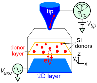 |
| If the atoms are close together compared to their effective Bohr radius (a few nanometers), the stong interaction alters the quantum structure of electrons trapped on the donors. Systems such as this can be regarded as "molecules" of donor atoms, providing a testing ground for fundamental questions of molecular physics. Moreover, we can investigate how deliberate changes in the local electronic environment, such as the addition of applied electric fields, can perturb the quantum levels in coupled systems. |