In 1821, Thomas Seebeck observed that an electric current would flow continuously
in a closed circuit made up of two dissimilar metals, if the metals were at
different temperatures. Thus Seebeck discovered that electricity and the flow of
thermal energy are closely connected. New nano-engineered materials have emerged with
outstanding potential for greater thermoelectric performance. For these materials,
understanding the effects of quantum confinement and the role played by defects
is key. For example, many of the new materials are based on a quantum architure approach
using bismuth telluride and bismuth selenide as the basic building blocks.
Our research is focused on applying scanning probe techniques to test the
basic physics at play in these systems.
The project involves a close collaboration with theoretical professor
Prof. S.D. Mahanti.
The figure below shows an example
of our recent work.
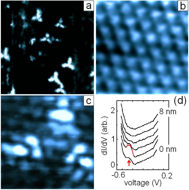
(a) A 25 x 25 nm scanning tunneling microscopy image of a Bi2Se3 doped with excess bismuth. Striking clover shaped features are clearly present.
(b) A 3.5 x 3.5 nm atomic resolution image of a similar sample. We see the exposed surface of selenium atoms.
(c) A 3.5 x 3.5 nm image of the same area; this time the sample bias voltage is set near -0.5 V. We see an atomically resolved clover that clearly
reflect electronic structure (as opposed to toporgraphy). We believe
The feature reflects the way the surface electronic structure is
perturbed by a subsurface defect. In this case, a
Bi substitution 5 atomic layers below the surface gives rise
to a resonant state that preferentially follows along chains of
atomic p-orbitals. (d) Differential conductance spectra sampled
at various distances from the center of the clover along one
of the three leaves. The peak (red) is the resonance that forms the clovers. The horizontal axis gives
the energy of the state with respect to the Fermi level.