1. Using the tight-binding method and assuming spherically symmetric wave functions and only nearest-neighbor interactions:
(a) (3 pt.) Find the expression E(k) for the simple cubic, bcc, and fcc crystal structures.
(b) (1 pt.) Find the expression E(k) for a two-dimensional square lattice.
(c) (1 pt.) Plot E(k)=const. in the first BZ in (b). Discuss the relation to the Fermi surface.
(In a, b, and c, treat the hopping integral γ as a parameter.)
2.
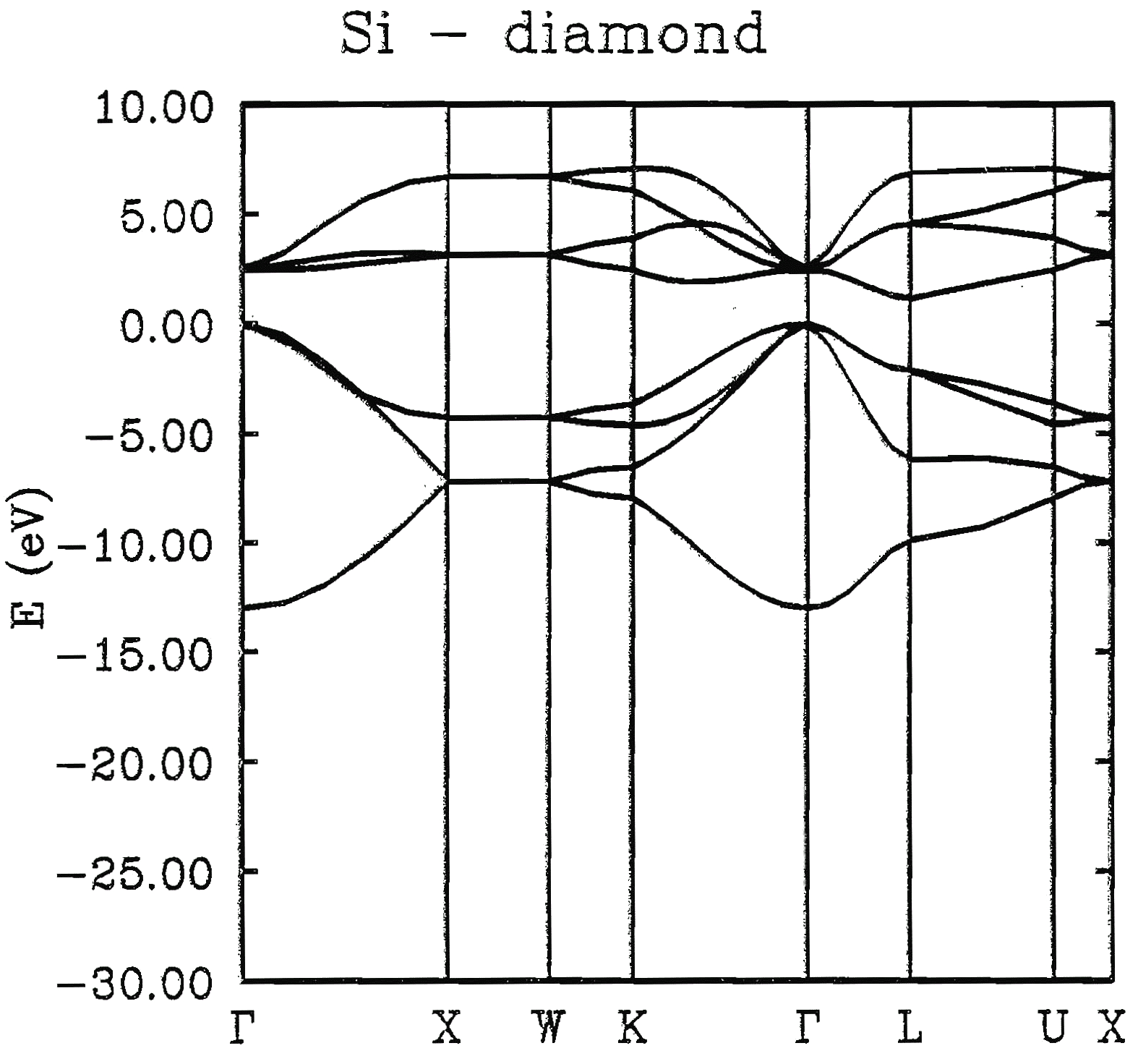
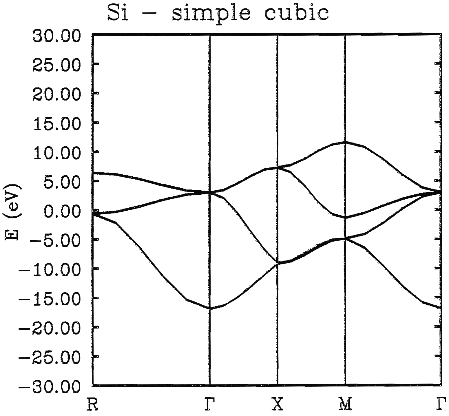
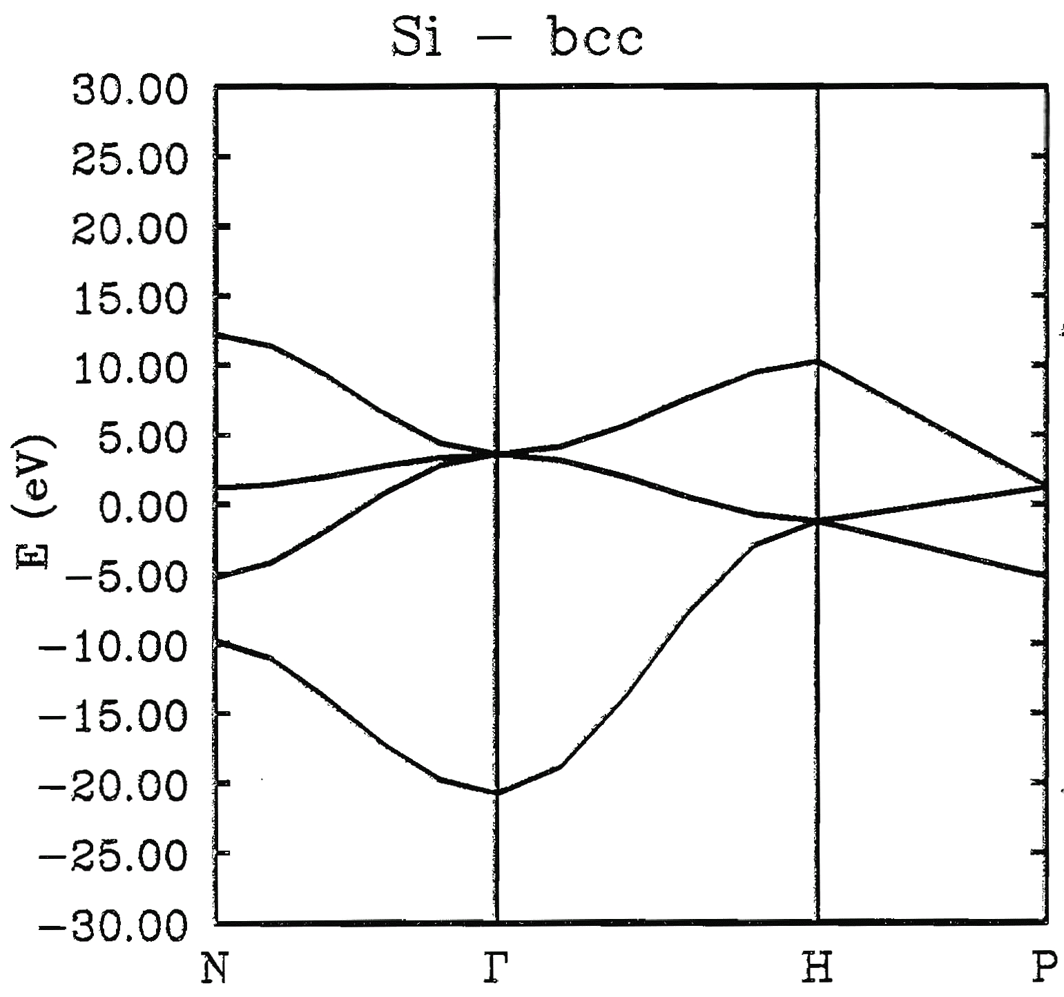
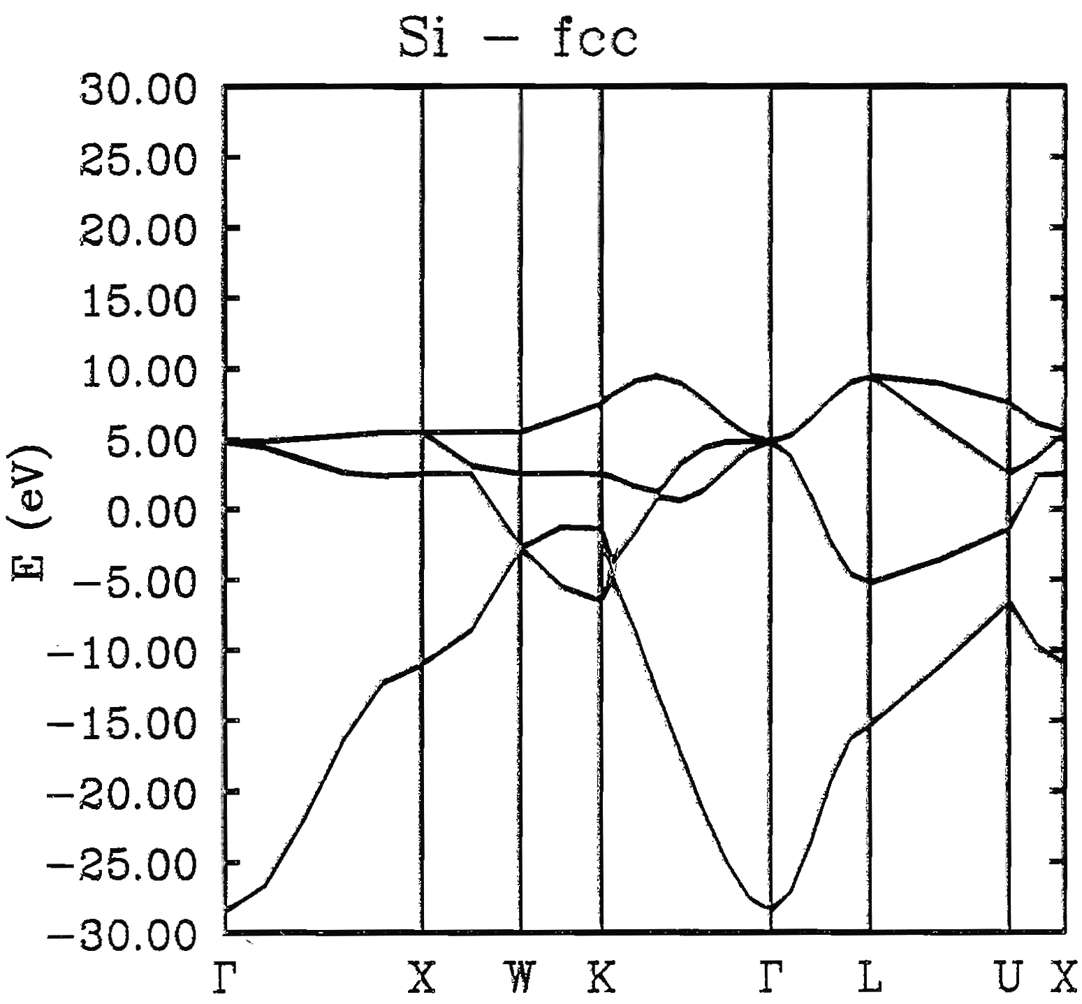
A young Physicist performed tight-binding calculations for different Si
lattices, setting the position of the Fermi level at E=0, and obtained
the following results:
(a) (2 pt.) Which of the fcc, bcc, simple cubic and diamond structures of silicon is metallic and which is a semiconductor?
(b) (2 pt.) Find the bandwidth and the width of the band gap(s) for each structure. Is the bandwidth correlated with the coordination number?
(c) (2 pt.) Identify valence and conduction bands in the semiconducting structure(s). Find the k-points corresponding to the top of the valence band and the bottom of the conduction band. Compare to published results.