


A lot of research in solid state physics and materials science are driven by the discovery of novel materials with reduced dimensions, such as van der Waals layered materials, nanowires, and quantum dots. On the one hand, the utility of engineered low-dimensional materials for important applications such as energy conversion and storage devices, nanoscale electronics, and molecular/biological sensors has in many cases been severely limited by interfacial phenomena that emerge at the nanoscale. On the other hand, new functionalities and exotic behaviors that are not accessible in individual constituents may arise from interfacial proximity coupling when low-dimensional materials of different properties are integrated into heterostructures. It is thus crucial to develop a thorough atomic- and molecular-level understanding and a precise control of surfaces and interfaces.
Our research group focuses on understanding the fundamental properties of low-dimensional electronic and photovoltaic materials using scanning probe microscopy in conjunction with device characterization, and furthermore manipulating the properties of these low-dimensional materials via surface and interface engineering. We utilize in-house growth facilities such as molecular beam epitaxy and ultrahigh vacuum chemical vapor deposition to fabricate these low-dimensional materials and heterostructures.
Areas of research:
1) Heterostructures of FeSn Kagome metal
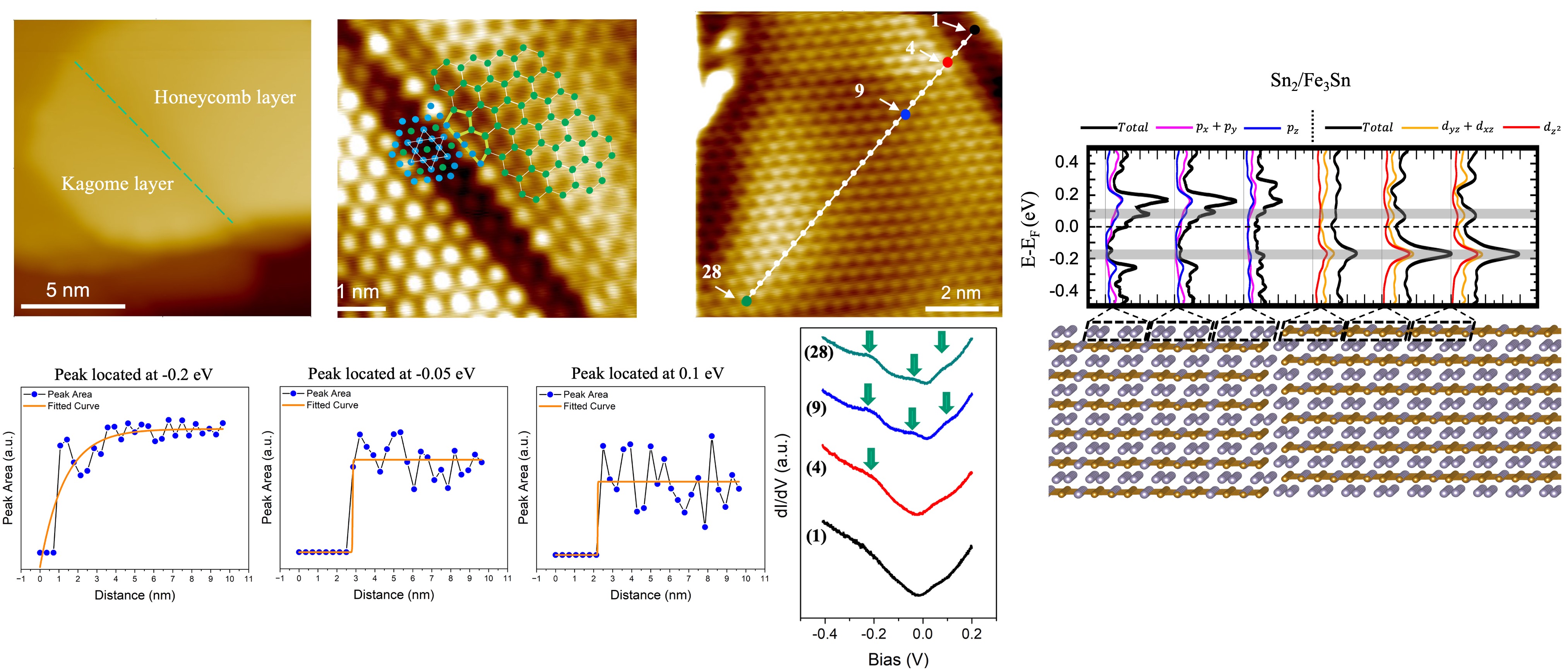
ACS Nano 18, 8768 (2024).
2) Lateral heterostructures of metal dichalcogenides
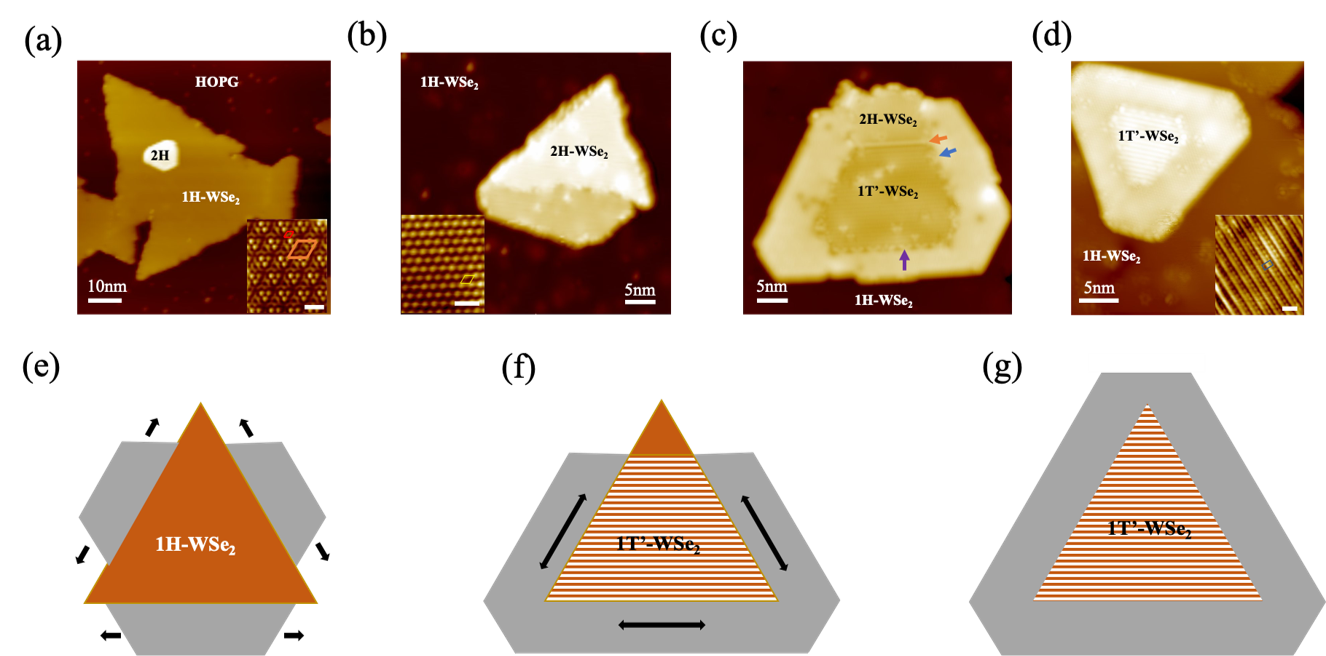
Materials Horizons 8, 1029 (2021).
3) Thin films of organic charge transfer complexes
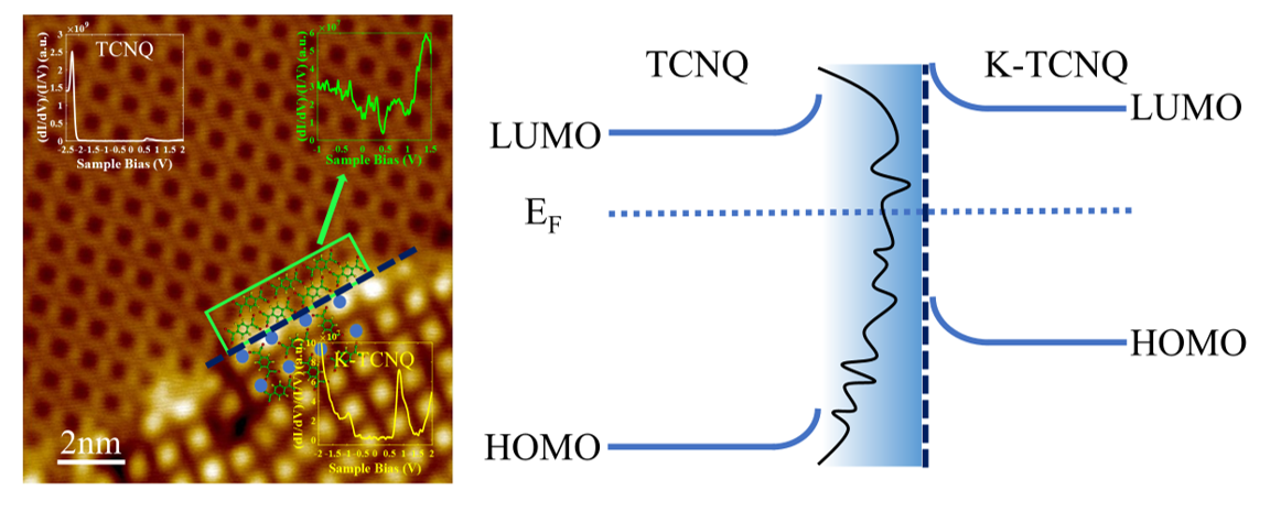
J. Phys. Chem. Lett. 11, 8352 (2020).
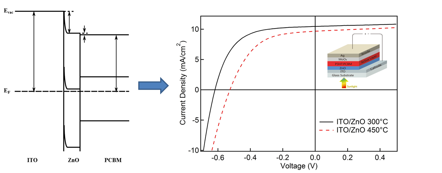
4) Hetero-interfaces between organic and inorganic materials
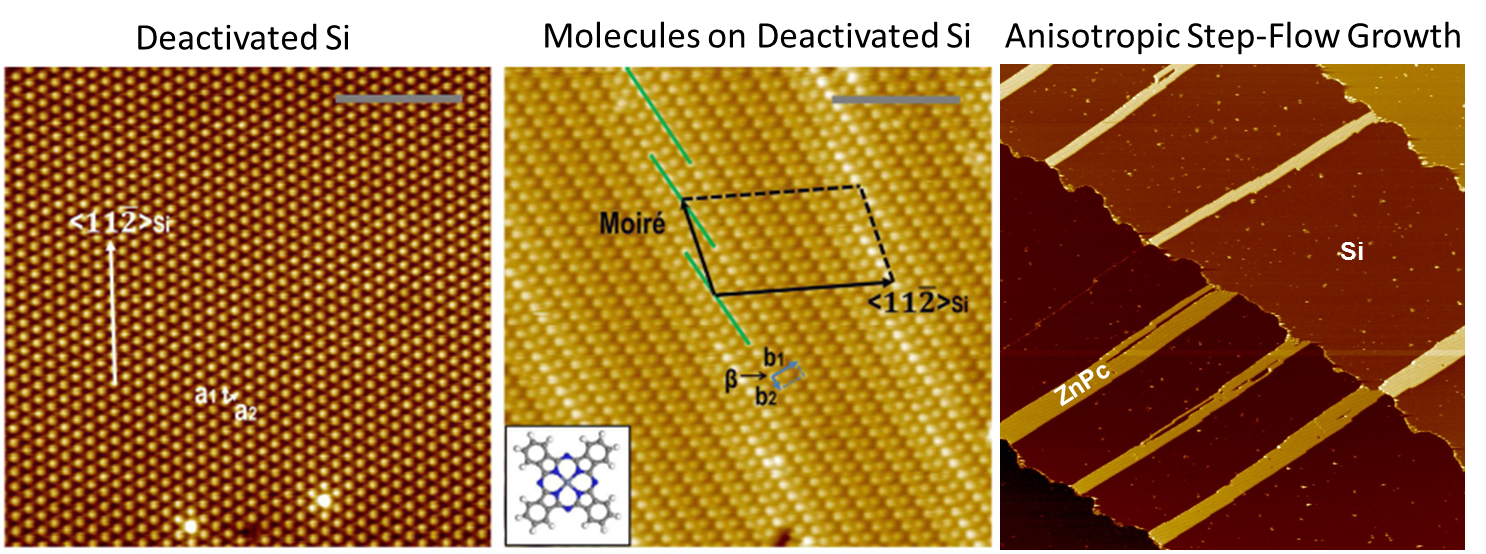
Phys. Rev. Lett. 110, 086107 (2013); Phys. Rev. Lett. 115, 096101 (2015).
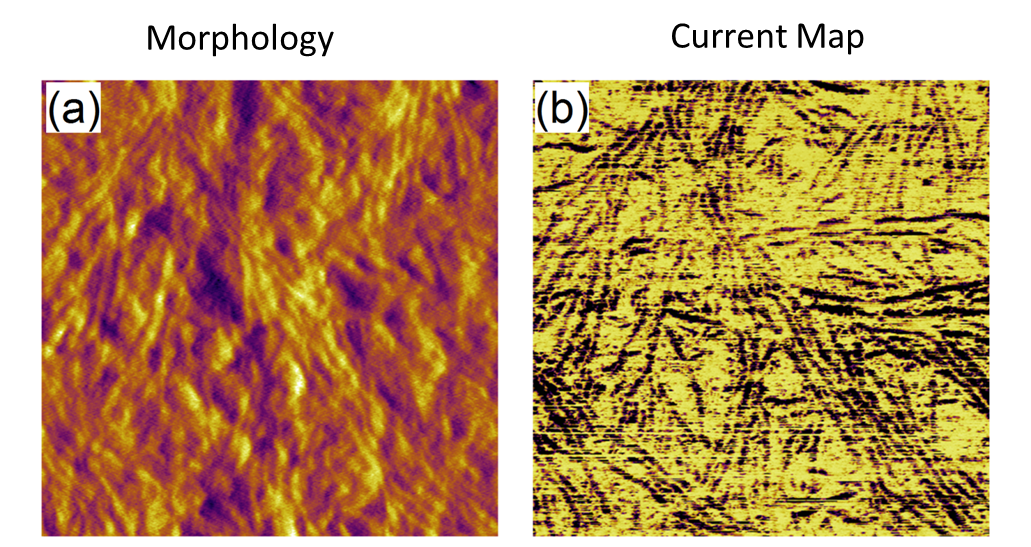
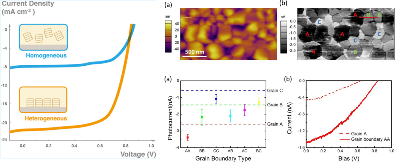
5) Scanning probe applications on functional materials and nanostructured devices
Org. Electron. 15, 441 (2014).
RCS Adv. 4, 3604 (2014).
ACS Omega 3, 3522 (2018); J. Appl. Phys. 123, 083105 (2018).