|
|
|
|
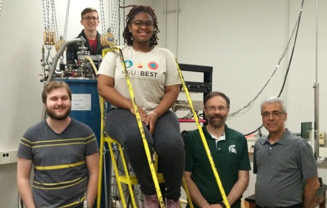
| Nano Group, June 2017. Left to right: Michael Gottschalk (grad), Eric Goodwin (grad), Ashlee Gordon (undergrad SROP), Tessmer, Dr. Reza Loloee (Materials Science Specialist). |
| We develop and apply low-temperature scanning probe
techniques to study the behavior of charges in nanoscale
systems. The techniques include Scanning Tunneling Microscopy and Charge Imaging -- a novel low temperature probe of
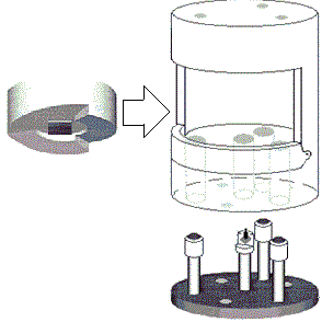
electron accumulation. The method achieves an incredible sensitivity of 0.01 electrons per root hertz. The picture to the right shows our custom-built cryogenic scanner. Current projects include probing electrons in superconductors and topological insulators and semiconductor structures. Superconductors and topological insulators are both materials that exhibit surprising and subtle behavior of charge and spin. When these materials are brought into contact spectacular effects can result, including the formation of Majorana fermions bound states.
The logo picture at the top left of this page shows an experiment published in Nature Physics and Nano Letters. Here we detected individual electrons entering small clusters of acceptor (dopant) atoms below the surface of a silicon semiconductor. The schematic shows a gray metallic tip positioned above two closely-spaced dopant atoms, represented as potential wells. If the atoms are close together compared to their effective Bohr radius (a few nanometers), the interaction alters the quantum structure of holes trapped on the acceptors. In this way, the study demonstrated that we can probe the smallest possible semiconductor devices -- composed of one or more individual dopant atoms. The research described on this site was supported by grants from the National Science Foundation (DMR-0906939, MCB-1021948), the MSU Foundation (Strategic Partnership Grant), the MSU Institute for Quantum Sciences and the Alfred P. Sloan Foundation. |
 |
The background pattern is an artist's view of atomic-scale three-leaved clovers -- formed by the electronic structure of selenium atoms on the surface of Bi2Se3, a narrow-gap semiconductor (paper). The pattern results from the interaction between the surface and a subsurface substitutional defect. The study was carried out by Tessmer's first grad student (now Professor), Sergei Urazhdin. |  |