
Department of Physics and Astronomy
Michigan State University
East Lansing, MI 48824-1116
Phone: (517) 884-5633
E-mail: mahanti@pa.msu.edu
Secretary: Ms. Cathy Cords
Phone: (517) 884-5512. Fax: (517) 353-4500.
Research Highlight
Effect of intrasite Coulomb interaction on the properties of pseudo-gap systems containing transition metals, Fe2VAl.
Phys. Rev. B 84, 125104 (2011)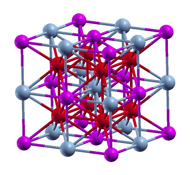
 Heusler compound Fe2VAl has been studied ab initially using DFT. The effect of intrasite Coulomb interaction is found important. The system is shown as narrow gap semiconductor instead of pseudo gap system as believed before.
*(a) GGA (b) GGA+U (c) mBJ (d) PBE0
Gap formation in Cu3SbSe4
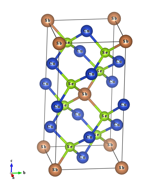
 It is found that the gap formation in Cu3SbSe4 is sensitive to non-local exchange interaction and the structure relaxtion. The gap is found of 0.26 eV using HSE06 in very good agreement with experimental value of the band gap.
Surface effects in layered semiconductors Bi2Se3 and Bi2Te3
Phys. Rev. B 69, 085313, (2004).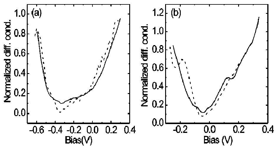 Solid lines: near-gap tunneling differential conductance dI/dVB spectrum of Bi2Se3, acquired directly with a lock-in detection technique at a temperature of 4.2 K. Dashed lines: theoretical curves. The curves are normalized by the differential conductance at VB=0.3V. (b) same as (a), for Bi2Te3.
Surface effects in layered semiconductors Bi2Se3 and Bi2Te3
Phys. Rev. B 69, 085313, (2004).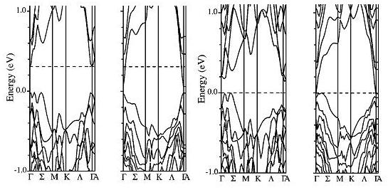 Calculated band structure using DFT (GGA) using slab geometry: (a) bulk Bi2Se3, (b) three layer slab of Bi2Se3, (c) bulk Bi2Te3, (d) three-layer slab of Bi2Te3. The experimental Fermi energies are shown in dashed lines; zero energy corresponds to the top of the valence band. The linearly dispersing bands inside the gap seen in slab calculations are topologically protected surface states (Dirac cones).
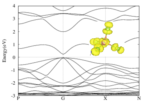
Deep Defect States in Narrow Band-Gap Semiconductors: In impurities in PbTe
Phys. Rev. Lett. 96, 056403, (2006).Phys. Rev. B 76, 115432, (2007).
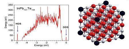
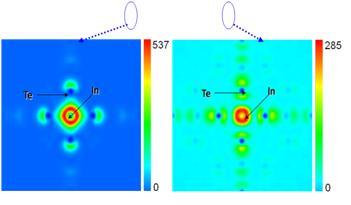
Total density of states of PbTe with In impurity calculated using a cluster model. There are two types of defect states, Hyper-Deep Defect (HDS) and Deep Defect (DDS) states and their charge distribution.
Frustrated Charge Neutral Yukawa lattice gas on a FCC lattice
He Huang and S. D. Mahanti (PhD thesis of He Huang, Michigan State University, 2011)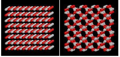
Frustrated Charge Neutral Yukawa lattice gas on a FCC lattice
He Huang and S. D. Mahanti (PhD thesis of He Huang, Michigan State University, 2011)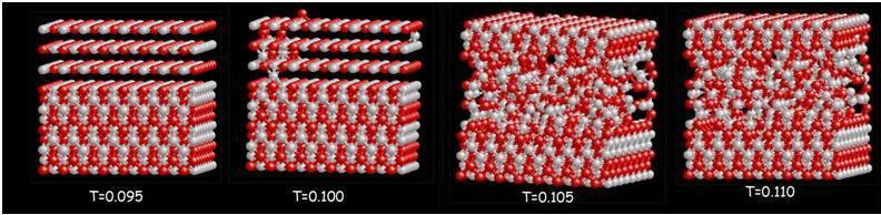 Melting ("Solid"-"Liquid") of a Charge Neutral Frustrated Yukawa Lattice Gas on a FCC lattice; x = 0.75 means that 75 % of the lattice sites are occupied by charges. T is the reduced temperature.
Before melting, "Solid"-structure (T = 0.095) is built up by two parts, one part is of x = 1 and the other is of x = 0.5. Melting process is inhomogeneous, starting in the x = 0.5 region eventually percolating the entire system.
Melting ("Solid"-"Liquid") of a Charge Neutral Frustrated Yukawa Lattice Gas on a FCC lattice; x = 0.75 means that 75 % of the lattice sites are occupied by charges. T is the reduced temperature.
Before melting, "Solid"-structure (T = 0.095) is built up by two parts, one part is of x = 1 and the other is of x = 0.5. Melting process is inhomogeneous, starting in the x = 0.5 region eventually percolating the entire system.